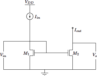
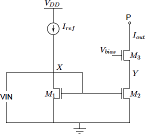
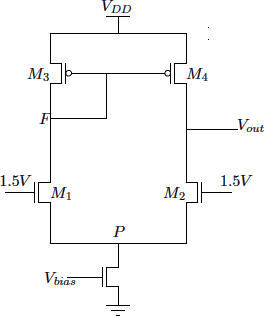
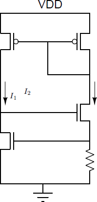
Common Data : VDD = 1.8V , Lmin = 0.18µm, µ0N = 350cm2/V s, µ0P = 100cm2/V s, |VTH | = 0.55, tox = 3.8nm, λ = 0.07V−1, χ = 0.1.
For the curved surface of the cylinder, the unit vector is ![]() which gives
which gives ![]() Parameterize
Parameterize ![]() ,Since we are confined to the first octant
,Since we are confined to the first octant ![]() The flux through the slant surface is
The flux through the slant surface is ![]() . The top and the bottom caps are in the
. The top and the bottom caps are in the ![]() directions, the contribution from these two give zero by symmetry. There are two more surfaces if we consider the first octant, they are the positive x-z plane and the positive y-z plane., the normal to the former being in the direction of
directions, the contribution from these two give zero by symmetry. There are two more surfaces if we consider the first octant, they are the positive x-z plane and the positive y-z plane., the normal to the former being in the direction of ![]() while that for the latter is along
while that for the latter is along ![]() directions. The flux from the former is
directions. The flux from the former is ![]() , while that from the latter is
, while that from the latter is ![]() . Adding up all the contributions, the total flux from the closed surface is zero. This is consistent with the fact that the divergence of the field is zero.
. Adding up all the contributions, the total flux from the closed surface is zero. This is consistent with the fact that the divergence of the field is zero.


